DNA Templates
ASCENT’s objective in this project is to use DNA to create nanometer-scale shapes for forming integrated circuit structures. The molecules will be assembled using a “DNA origami” technique [1] in which a longer, single strand of DNA is held into shape with many shorter, complementary strands. The DNA assemblies will be formed in solution, chemically directed to a targeted place on a surface, and then metallized to form conductive components of a circuit. We have completed the design of a model DNA object for initial tests in making nanoscale structures using this origami technique. This rectangular shape will be formed from a lambda DNA restriction fragment and 24 custom-synthesized oligonucleotides. Fig. 1 shows a structural model of this ~8 x 60 nm DNA object. Fig. 2 demonstrates how three oligonucleotide strands in the structure can be replaced to provide “sticky ends” to facilitate (1) larger-scale assembly of one-dimensional arrays or (2) chemically-directed surface assembly of DNA rectangles. Future efforts will focus on forming more complex two-dimensional DNA objects. These objects can serve as circuit templates that will be metallized to form multiple electrical leads which can then connect to active nanostructure circuit elements.
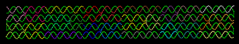
Figure 1. Structural model of a prototype nanoscale object showing individual DNA segments as different colors.
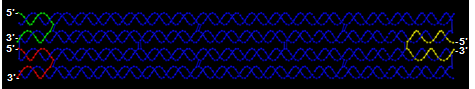
Figure 2. DNA structural model indicating three shorter strands that can be modified to provide “sticky ends” for larger-scale assembly.
Go to top
High-resolution Chemical Surface Patterning
One of the primary goals of the ASCENT project is nanoscale chemical surface patterning. We are in the process of developing a scanning probe lithography technique that allows for patterning of adsorbed, water-soluble polymers on functionalized oxide surfaces to serve both as a path for nanowire plating and as a possible method for the placement of DNA templates. SiO2 and borosilicate glass surfaces are functionalized with an organosilane monolayer of known surface charge. A ~2 nm polymer layer of opposite electric charge is then deposited over the silane film. An atomic force microscope (AFM) probe is used to scribe away patterns in the polymer, exposing the silane underlayer. Patterned regions have been backfilled with a fluorescently tagged polymer and were characterized using optical fluorescence microscopy. An overview of the process is shown in Fig. 3 below.
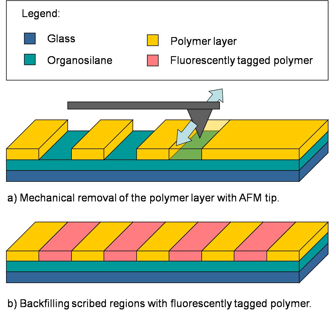
Figure 3: Overview of the surface patterning process.
The AFM scribing experiments have been successfully performed both in air and in water and were characterized using tapping mode AFM. AFM height and phase mode data showed lines and spaces with half pitch features as small as 12 nm, showing that the process is capable of the spatial resolution needed for nanowire fabrication. Furthermore, the process is fully capable of operating in the native aqueous chemistry of DNA. Figure 4 shows an example of chemical changes (indicated by fluorescence) that can be effected with this method.
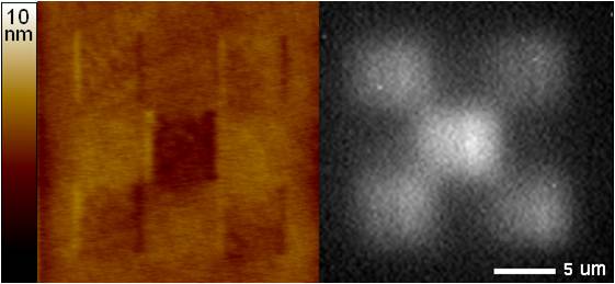
Figure 4: Tapping Mode AFM height image (left) and fluorescence micrograph (right) of a five box pattern.
Chemical Control and Versatility
Although we performed the nanoshaving in air, all steps in aqueous polymer nanografting can be performed in aqueous environments where pH and concentration can be controlled, making it compatible with patterning sensitive biological molecules. This technique can also be used to pattern multiple polymers on one surface with different chemical functionalities.
Go to top
Metallization
Our aim in this area is to provide selective metallization of DNA templates for the formation of nanoelectronic devices and connection of those devices to other circuit elements. Several different plating systems were examined this year. Of these, silver deposition showed the most promise. Hence, a key objective of our metallization work this year was to understand the formation process of silver nanowires on DNA templates and use that method to fabricate silver nanowires with sub-20 nm size.
Plating is typically performed in two major steps: 1) seed formation and 2) deposit growth. For the seeding process, we aligned DNA on an octyldimethylchlorosilane-passivated surface first, rinsed the surface with nanopure water and then dried the surface with a nitrogen stream. Next, we placed a droplet of silver nitrate solution (pH adjusted by NH4OH) on the surface and for a minimum of 5 minutes to allow the silver ions to associate with the DNA. Then, the droplet was removed by a stream of nitrogen. Finally, a hydroquinone solution was used to reduce the silver ion.
We found that silver formed nanoparticles on DNA templates with heights of several nanometers (Fig. 8). The figure clearly shows that the silver particles selectively bind to DNA templates and form a chain-like structure. Rather than use a separate deposition solution, we repeated the seeding process and were able to produce more continuous wires. The average height of silver nanowires in the image below is 13.5 nanometers (Fig. 3). An approximate material balance indicated that the amount of silver deposited was significantly greater than what was expected to be directly associated with the DNA. We think that the source of additional silver might have been residual silver on the surface that was not associated with the DNA. High resolution XPS will be performed to verify this hypothesis.
For some samples, electroless silver plating in a separate bath was performed on the seeded templates to form larger more continuous nanowires.
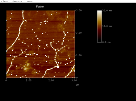
Figure 8: AFM height image of silver nanowires formed on DNA templates.
Go to top
Directed Assembly and Integration
Year 1 efforts in the area of assembly and integration were focused on carbon nanotube alignment and selective placement in nanowire gaps. Dielectrophoresis is a promising technique for controlling placement of carbon nanotubes. When an AC-electric field is applied between two electrodes, carbon nanotubes in the region are polarized and attracted to the highest gradient in the region [2, 3]. It has been shown that placement of one carbon nanotube can inhibit other carbon nanotubes from attaching nearby. Also, these carbon nanotubes – when placed by dielectrophoresis – can survive standard lithographic processing [4]. Dielectrophoresis has recently been used by others to place metallic carbon nanotubes as interconnects for silicon CMOS transistors. Electrode spacing in prior work has been performed on the on the scale of one to several microns. Here we explore the placement of purified semiconducting carbon nanotubes on nanometer-scale electrode geometries.
Nanotubes were purified using ultracentrifugation as reported by Crochet et al. [5] to obtain semiconducting nanotubes. Spectrophotometry was used to verify separation of semiconducting and metallic tubes. In our initial electrophoresis deposition we observed a large fraction of aligned carbon nanotubes on the surface between electrodes (See Figs. 9 and 10). This result is likely due to the large electric field we are using. These aligned semiconducting nanotubes should be compatible with our target nanoscale devices by careful electrode geometry design. We are also exploring selective placement of the nanotubes in nanogaps but currently see a large adsorption background. To reduce this background we are experimenting with silane surface treatments to reduce non-selective adsorption. Our initial surface treatment efforts have reduced background absorption by 50 percent.
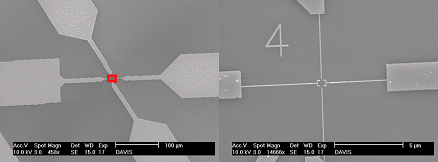
Figure 9: Device made by e-beam lithography to mimic the DNA- templated circuit.
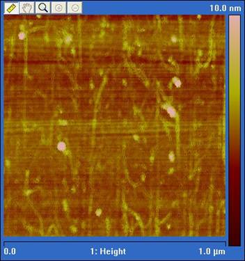
Figure 10: Carbon nanotubes aligned using dielectrophoresis.
Go to top
References
[1] Rothemund, P. W. K. Folding DNA to create nanoscale shapes and patterns. Nature, 440, 297-302 (2006).
[2] H. A. Pohl, “The Motion and Precipitation of Suspensiods in Divergent Electric Fields,” Journal of Applied Physics 22, 869-871 (1950).
[3] T. Schwamb, T.-Y. Choi, N. Schirmer, N. R. Bieri, B. Burg, J. Tharian, U. Sennhauser, and D. Poulikakos, “A Dielectrophoretic Method for High Yield Deposition of Suspended, Individual Carbon Nanotubes with Four-Point Electrode Contact,” NanoLetters 7, 3633-3638 (2007).
[4] M. R. Diehl, S. N. Yaliraki, R. A. Beckman, M. Barahona, and J. R. Heath, “Self-
Assembled, Deterministic Carbon Nanotube Wiring Networks,” Angew. Chem. Int.
Ed. 41, 353-356 (2002).
[5] J. Crochet, M. Clemens, and T. Hertel, “Quantum Yield Heterogeneities of Aqueous
Single-Wall Carbon Nanotube Suspensions,” Journal of the American Chemical Society 129, 8058-8059 (2007).